TL;DR
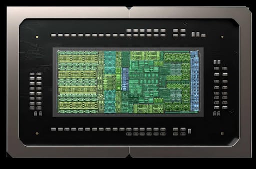
GB10, a Nvidia–Mediatek SoC that brings Blackwell GPU cores into an integrated package, pairs 20 Arm CPU cores with a layered cache and LPDDR5X memory system that balances latency and bandwidth. The chip splits its CPUs into two asymmetric clusters with differing L3 capacity and external bandwidth, producing tradeoffs in latency under load and overall data-sharing behavior between CPU and GPU.
What happened
Nvidia and Mediatek’s GB10 integrates a 48-SM Blackwell GPU with a 20-core Arm CPU complex split into two clusters. Each cluster contains five Cortex A725 and five Cortex X925 cores; A725 cores run at 2.8 GHz while X925 clocks reach 3.9–4.0 GHz depending on cluster. Cache sizing choices include 64 KB L1 I/D per core, 512 KB L2 for each A725 and 2 MB L2 for each X925. Cluster 0 provides an 8 MB shared L3 whereas Cluster 1 exposes 16 MB of L3; measured L3 latencies differ between core types (A725 sees >21 ns, X925 around 14 ns). A 16 MB system-level cache sits after L3 and serves as an L4/cache for cross-engine sharing with measured latencies near the tens of nanoseconds. Measured DRAM latency is approximately 113 ns for LPDDR5X, and reported memory speeds vary up to 9,400 MT/s (Hot Chips) with dmidecode showing ~8,533 MT/s. Bandwidth measurements show higher per-core L3 and DRAM throughput from X925 cores versus A725, while aggregate L3 bandwidth exceeds 200 GB/s.
Why it matters
- Cache and cluster design strongly shape single-thread and multithreaded responsiveness on GB10, affecting real-world CPU performance.
- The system-level cache (16 MB) enables CPU–GPU data sharing without round trips to DRAM, which can improve power efficiency for heterogeneous workloads.
- Asymmetric clusters and differing external interfaces create tradeoffs between die area, latency, and sustained bandwidth that impact scheduler and power management strategies.
- LPDDR5X memory speeds and on-die memory controller proximity help lower DRAM latency compared with other mobile-class designs, influencing mobile SoC responsiveness.
Key facts
- GB10 pairs 48 Blackwell GPU SMs with a 20-core Arm CPU complex (10 Cortex X925 + 10 Cortex A725).
- Each core uses 64 KB L1 instruction and 64 KB L1 data caches.
- A725 cores have 512 KB L2 (8-way, ~9 cycle latency ≈ 3.2 ns); X925 cores have 2 MB L2 (8-way, ~12 cycle latency).
- Cluster 0 has 8 MB L3; Cluster 1 has 16 MB L3. A725 L3 latency measured >21 ns (>60 cycles); X925 L3 latency ~14 ns (~56 cycles).
- A 16 MB system-level cache (L4) sits after L3 with latency measurements roughly 42–47 ns depending on core.
- Measured DRAM latency ≈ 113 ns for LPDDR5X; Hot Chips slides quote up to 9,400 MT/s and dmidecode reports ~8,533 MT/s.
- Per-core bandwidth: A725 reads L1 at 48 B/cycle and reaches ~55 GB/s from L3; X925 reads L1 at 64 B/cycle and reaches ~90 GB/s from L3.
- Single-core DRAM bandwidth: ~26 GB/s for A725, ~38 GB/s for X925.
- Aggregate L3 bandwidth is reported north of 200 GB/s; Cluster 1 offers over 100 GB/s read bandwidth externally.
- The CPU clusters are built on Arm’s DSU-120 and may use multiple CHI interfaces, which could explain asymmetric external bandwidth.
What to watch next
- Whether Nvidia/Mediatek or future GB10 firmware changes expose cluster specialization or scheduler hints to improve workload placement (not confirmed in the source).
- Any shipping devices’ final LPDDR5X speed and thermal behavior compared with the Hot Chips and dmidecode figures (not confirmed in the source).
- How OS schedulers adapt to the asymmetric L3 and external bandwidth characteristics versus a homogeneous-cluster approach (not confirmed in the source).
Quick glossary
- System-Level Cache (SLC): A shared cache positioned after the CPU L3 that can act as an L4 cache and help different engines on the chip share data without accessing DRAM.
- L1/L2/L3 cache: Hierarchical on-chip memories with decreasing speed and increasing capacity: L1 is fastest and smallest, L2 is larger and slower, and L3 is larger still and shared across cores.
- LPDDR5X: A low-power DDR memory standard commonly used in mobile and integrated SoCs, offering high bandwidth at reduced power compared with older mobile DRAM types.
- Bandwidth vs. Latency: Bandwidth is the amount of data transferable per unit time; latency is the time a request takes to complete. Designs trade between high throughput and low individual-request delay.
- CHI (Coherent Hub Interface) and DSU-120: CHI is an Arm coherence/interconnect protocol; DSU-120 is Arm’s DynamIQ Shared Unit used to compose CPU clusters and attach coherent interfaces.
Reader FAQ
How many CPU cores and what types are in GB10?
GB10 uses 20 Arm cores: ten Cortex X925 and ten Cortex A725, split into two clusters of five of each core per cluster.
What is GB10’s shared cache configuration?
Clusters differ: Cluster 0 exposes 8 MB of L3 while Cluster 1 has 16 MB of L3; a 16 MB system-level cache sits after L3.
Does GB10 use LPDDR5X and how fast is the memory?
Measured DRAM latency is about 113 ns for LPDDR5X; Hot Chips slides cite up to 9,400 MT/s and dmidecode reports ~8,533 MT/s.
Do the clusters have identical external bandwidth?
No — testing indicates asymmetrical external bandwidth between the two CPU clusters.
Will GB10’s clusters be reorganized into homogeneous clusters?
not confirmed in the source
Inside Nvidia GB10’s Memory Subsystem, from the CPU Side CHESTER LAM DEC 31, 2025 6 2 Share GB10 is a collaboration between Nvidia and Mediatek that brings Nvidia’s Blackwell architecture…
Sources
- Nvidia GB10's Memory Subsystem, from the CPU Side
- Analysis of NVIDIA DGX Spark's GB10 SoC – Chip Log
- NVIDIA DGX Spark In-Depth Review: A New Standard for …
- NVIDIA Puts Grace Blackwell on Every Desk and at …
Related posts
- 2026: The Year Java Claims the Terminal – CLIs, TUIs and Tools
- Scaffolding to Superhuman: Curriculum Learning Beats 2048 and Tetris
- When square pixels aren’t square: why video pixel aspect ratio matters