TL;DR
At CES 2026 AMD previewed a next-generation AI stack: MI500-class accelerators, Helios rack systems built from MI455X chips, and a high-core-count Venice Epyc CPU. AMD claims up to 1,000x AI performance improvement over an MI300X node, but the company’s comparison and many technical specifics remain incomplete.
What happened
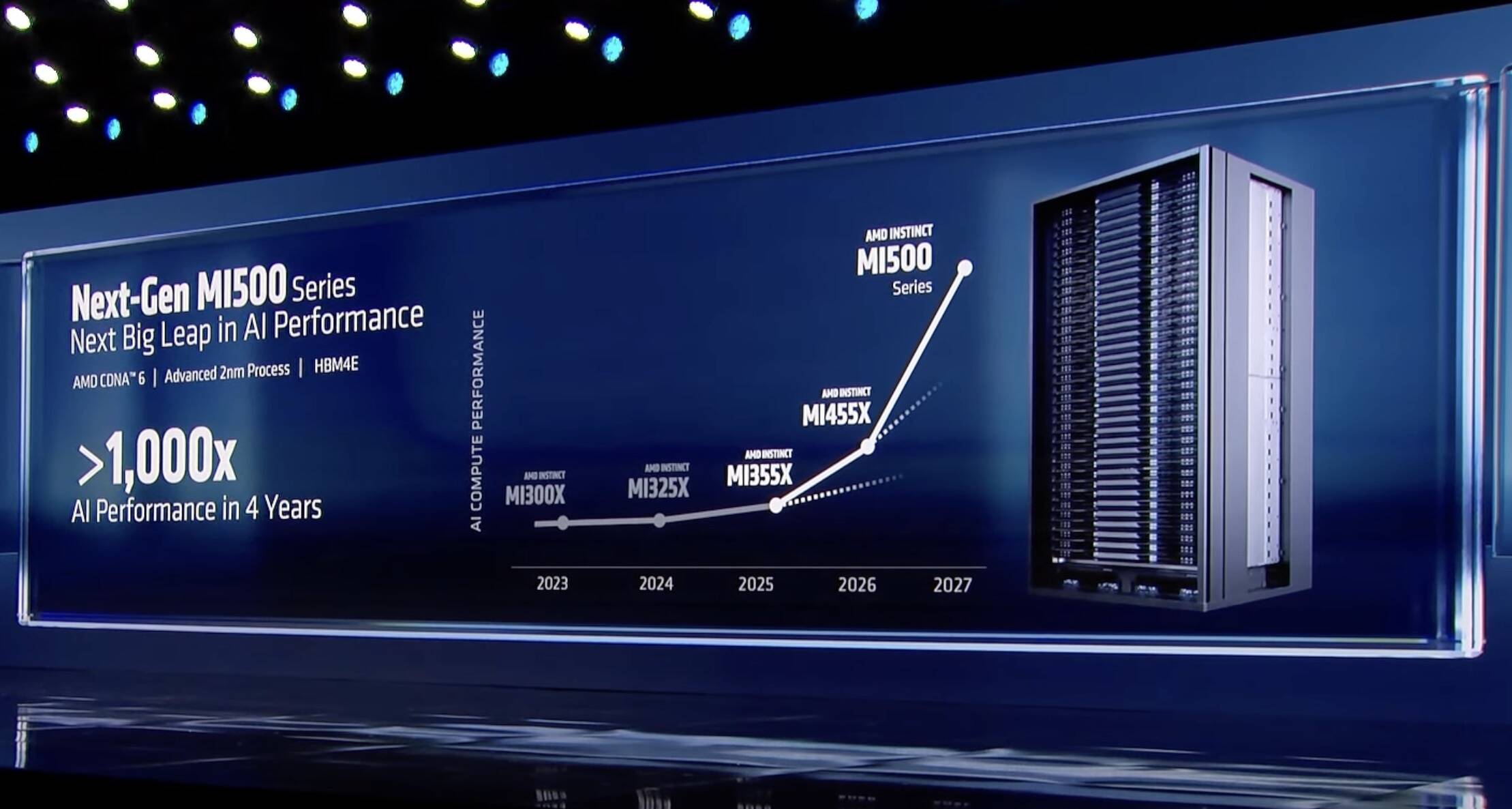
At CES 2026 AMD outlined a multi-part strategy to contest Nvidia in datacenter AI and HPC. The company touted an MI500 family of accelerators that it says will debut in 2027, built on TSMC process nodes (2 nm cited) and CDNA 6 architecture using HBM4e memory. AMD’s headline claim — a 1,000× performance uplift versus a two-year-old MI300X configuration — is framed as a comparison between an eight-GPU MI300X node and an unspecified MI500 rack, leaving the metric and GPU count unclear. More concrete details were provided for MI400-series parts and the Helios rack: the MI455X package shown onstage appears to use multiple 3D-stacked compute and I/O dies and what looked like twelve 36 GB HBM4 stacks. Helios racks will group 72 MI455X GPUs with Venice Epyc CPUs (one CPU per four GPUs) and use Pensando networking components and an open Ultra Accelerator Link interconnect over Ethernet.
Why it matters
- AMD is positioning full-stack hardware — GPUs, CPUs and networking — to directly compete with Nvidia in rack-scale AI systems.
- If realized, the MI500 family and Venice Epyc could change procurement choices for hyperscalers and enterprises seeking on-premise alternatives to cloud GPUs.
- Helios’s rack design emphasizes high memory bandwidth and dense GPU aggregation, addressing workloads that rely on interconnect and memory throughput as much as raw FLOPS.
- Claims about 1,000× gains underscore how headline metrics can obscure differences in test conditions, node configuration and workload types.
Key facts
- AMD announced a next-generation MI500 GPU family that it says will ship in 2027 and use CDNA 6 and HBM4e; the MI500’s detailed specs were not disclosed.
- AMD cited a 1,000× performance improvement versus MI300X, but this compares an eight-GPU MI300X node to an unspecified MI500 rack configuration.
- MI400-series variants revealed: MI455X (AI-optimized), MI440X (lower-end, eight-way boxes) and MI430X (mixed AI/HPC).
- The MI455X package shown included multiple 3D-stacked compute and I/O dies and what appeared to be twelve 36 GB HBM4 stacks.
- Helios racks are built from 72 MI455X GPUs with one Venice Epyc CPU for every four GPUs, and will use Pensando network/NIC components.
- AMD quoted per-chip figures for MI455X: ~40 petaFLOPS dense FP4 inference, ~20 petaFLOPS FP8 training, 432 GB HBM4, ~19.6 TB/s memory bandwidth and ~3.6 TB/s chip-to-chip interconnect (as presented at CES).
- A full Helios rack was described as delivering roughly 2.9 exaFLOPS dense FP4, 1.4 exaFLOPS FP8, 31 TB of HBM4 and ~1.4 PB/s memory bandwidth.
- Venice Epyc previewed with up to 256 Zen 6 cores in a packaging layout that appeared to show eight 32-core CCDs plus two I/O dies; AMD says Venice will offer double memory and GPU bandwidth over the prior generation.
What to watch next
- Exact GPU count and configuration used to produce AMD’s 1,000× MI500 performance claim — not confirmed in the source.
- Full MI500 chip microarchitecture, precision support (beyond FP4/FP8) and official FLOPS figures when AMD releases detailed specs.
- Shipping timeframe and availability for Helios racks and Venice Epyc SKUs across cloud, hyperscale and enterprise partners — not confirmed in the source.
Quick glossary
- FP4 / FP8: Low-precision floating-point formats used to accelerate AI inference and training by reducing memory and compute requirements compared with higher-precision formats.
- HBM4: Fourth-generation high-bandwidth memory that stacks memory dies to provide large capacity and very high bandwidth for accelerators and CPUs.
- Chiplet: A smaller integrated circuit module (chiplet) used together on a package to form a larger processor, enabling modular designs and heterogeneous integration.
- DPU (data processing unit): A programmable network or security accelerator that offloads tasks such as networking, storage and security from CPUs to improve overall system efficiency.
Reader FAQ
What did AMD claim about MI500 performance?
AMD said the MI500 family will provide up to a 1,000× uplift versus an eight-GPU MI300X node, though the comparison uses an unspecified MI500 rack configuration.
When will MI500 GPUs arrive?
AMD indicated MI500 will ship in 2027.
How many GPUs are in a Helios rack?
Helios racks are described as containing 72 MI455X GPUs paired with Venice Epyc processors (one CPU per four GPUs).
Does AMD provide full technical specs for MI500 today?
No. Many MI500 details, including chip-level FLOPS and the precise rack GPU count used for the 1,000× claim, are not confirmed in the source.
SYSTEMS AMD threatens to go medieval on Nvidia with Epyc and Instinct: What we know so far AMD boasts 1000x higher AI perf by 2027 and pulls the lid off…
Sources
- AMD threatens to go medieval on Nvidia with Epyc and Instinct: What we know so far
- AMD Expected to Break NVIDIA's AI Monopoly With Next-Gen Instinct …
- AMD teases nstinct MI500 GPUs, physical AI, Helios …
- AMD and its Partners Share their Vision for “AI Everywhere, …
Related posts
- T-Mobile launches ‘Better Value’ family plans and raises per-line fees in 2026
- Show HN: I visualized the entire Citi Bike history in-browser
- Roku says $3 streaming service Howdy will expand beyond Roku devices