TL;DR
MIT researchers built a fully autonomous robotic probe that images printed semiconductor samples, selects contact points using a domain-informed neural network, and maps photoconductance far faster than manual methods. In a 24-hour run the system made over 3,000 unique measurements (more than 125 per hour), revealing hotspots and degradation while reducing computation and path times versus other AI approaches.
What happened
A team at MIT has combined robotics, computer vision and machine learning to create a fully autonomous system that makes contact-based measurements of photoconductance on printed semiconductor samples. The robot first photographs a slide, segments the image, and feeds those segments into a neural network that incorporates materials-science expertise to pick informative probe contact points. A path-planning routine then computes an efficient sequence to visit those points; adding a small amount of randomness helped the planner find shorter routes. The system operates without labeled training data via a self-supervised model and drives the probe to take rapid successive readings. In a continuous 24-hour trial the setup logged more than 3,000 distinct photoconductance measurements at a rate exceeding 125 per hour, enabling detection of high-photoconductance regions and signs of material degradation. The work appears in Science Advances and is led by Tonio Buonassisi, with lead author Alexander Siemenn.
Why it matters
- Greatly speeds the characterization of contact-dependent material properties that are hard to measure without physical probing.
- Generates dense, high-resolution datasets that can reveal performance hotspots and early degradation in semiconductor samples.
- Bridges domain expertise and autonomous algorithms, improving repeatability and precision over manual measurements.
- Could shorten the development cycle for new semiconductors used in applications such as solar photovoltaics.
Key facts
- Property measured: photoconductance — the electrical response of a material to light.
- Workflow: onboard camera → image segmentation → domain-informed neural network → path planner → robotic probe contacts and measures.
- Machine-learning model is self-supervised and does not require labeled training data to select contact points.
- Path planner performance improved by adding small randomness to help find shorter routes.
- 24-hour autonomous experiment produced over 3,000 unique measurements, a rate above 125 measurements per hour.
- The neural network outperformed seven other AI-based methods for selecting contact points and required less computation time.
- System identified spatial heterogeneity including hotspots of higher photoconductance and areas of material degradation.
- Paper: “A Self-Supervised Robotic System for Autonomous Contact-Based Spatial Mapping of Semiconductor Properties” in Science Advances.
- Lead and senior authors: Alexander (Aleks) Siemenn (lead author) and Tonio Buonassisi (senior author); co-authors include Basita Das, Kangyu Ji, and Fang Sheng.
- Support and funding came from First Solar, Eni via the MIT Energy Initiative, MathWorks, the University of Toronto’s Acceleration Consortium, the U.S. Department of Energy, and the U.S. National Science Foundation.
What to watch next
- Further development toward a fully autonomous materials-discovery laboratory, as the team continues integrating this capability into broader workflows.
- not confirmed in the source: timeline or plans for industrial deployment or wide commercial adoption of the system.
- not confirmed in the source: application of the method to measurement of other contact-based material properties beyond photoconductance.
Quick glossary
- Photoconductance: A measure of how a material's electrical conductivity changes when it is illuminated.
- Perovskite: A class of crystalline materials often studied for use in photovoltaic cells and other optoelectronic devices.
- Self-supervised learning: A machine-learning approach where models learn from patterns in unlabeled data, deriving supervisory signals from the data itself.
- Path planning: An algorithmic process for finding an efficient route for a robot or probe to move between multiple target points.
- Computer vision: Techniques that enable machines to interpret and process visual information from images or video.
Reader FAQ
What property does the robotic system measure?
It measures photoconductance, the electrical response of a material to light.
How fast did the system collect data?
In a continuous 24-hour trial it gathered more than 3,000 unique measurements, averaging over 125 measurements per hour.
Is the system fully autonomous?
The system operated fully autonomously during the 24-hour experiment, though the team notes that human expertise remains important in the loop.
Was this tested on commercial solar panels?
not confirmed in the source
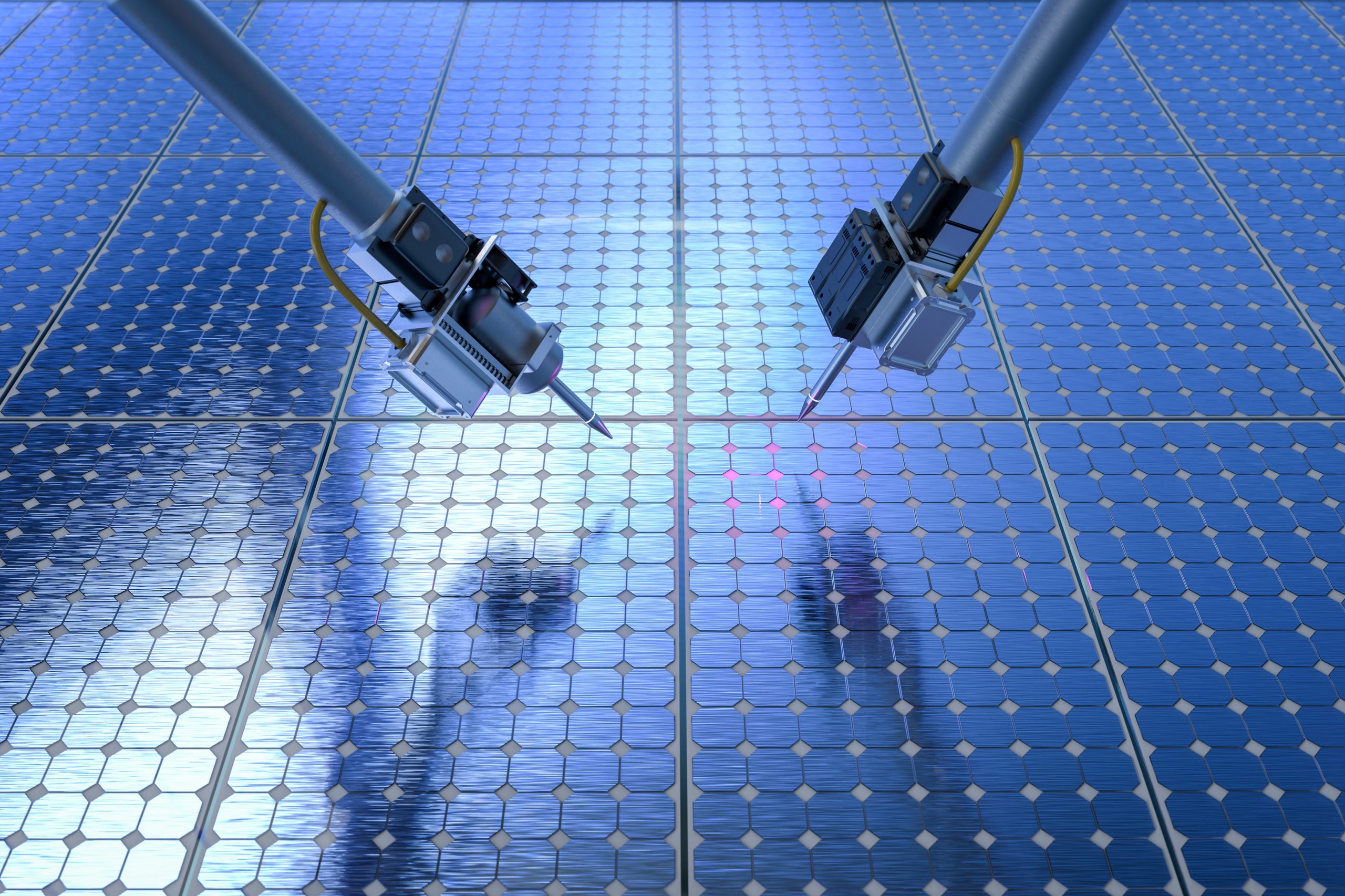
Developed to analyze new semiconductors, the system could streamline the development of more powerful solar panels. Adam Zewe | MIT News Publication Date : July 4, 2025 PRESS INQUIRIES Caption…
Sources
- Robotic probe quickly measures key properties of new materials
- A self-supervised robotic system for autonomous contact …
- MIT Researchers Develop Autonomous Robotic System for …
- MIT's new robot runs 3000 photoconductivity tests a day to …
Related posts
- MIT AI pipeline redesigns underwater gliders into new hydrodynamic forms
- PhysicsGen: Simulation-driven pipeline that tailors robot training data
- MIT handheld interface lets users teach robots with three demo modes