TL;DR
At CES 2026 AMD publicly displayed silicon for its forthcoming Venice EPYC server family and MI400 datacenter accelerators. The reveal highlighted new packaging approaches, larger IO die area on Venice, and a multi-die MI400 design with HBM4 memory and multiple compute and IO dies.
What happened
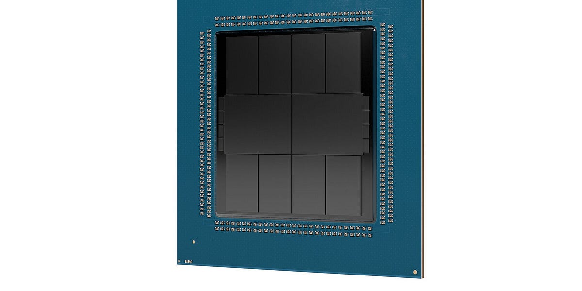
At CES 2026 AMD presented physical examples of two upcoming product lines: the Venice series of EPYC server SoCs and the MI400 family of datacenter accelerators. Venice was shown with eight chiplet CCDs and what appears to be two separate IO dies, using a more advanced package interconnect than AMD’s previous organic substrate approach. Measurements from the exhibited packages place each CCD at roughly 165 mm2 (N2), implying up to 256 cores per package if each CCD contains 32 Zen 6 cores. The IO dies look substantially larger than on prior EPYC designs, roughly 353 mm2 each. The MI400 display showed a large package with 12 HBM4 stacks plus a mix of 2 nm and 3 nm compute and IO dies; observers count two large base dies and additional off-package IO dies. AMD also confirmed new SKUs including the MI440X and a Venice-X variant, and said both Venice and the MI400 series are scheduled to launch later this year.
Why it matters
- Packaging changes on Venice suggest AMD is evolving inter-die connectivity and power delivery for higher core counts.
- Larger IO die area could enable expanded I/O and memory controller complexity, affecting platform capabilities and costs.
- MI400’s multi-die HBM4 design indicates AMD is scaling memory and compute density for AI/datacenter workloads.
- New SKUs (MI440X, Venice-X) signal AMD is targeting diverse server configurations, including UBB 8‑way systems and V-Cache variants.
Key facts
- Venice appeared with eight CCDs, each reportedly containing 32 cores, for up to 256 cores per package.
- Each Venice CCD was measured at about 165 mm2 on N2 process; estimate assumes Zen 6 cores.
- Venice showed two IO dies, each roughly 353 mm2, totaling just over 700 mm2 for IO silicon — larger than prior EPYC IO die allocations.
- Packaging for Venice seems to move away from an organic substrate to a more advanced interconnect approach similar to Strix Halo or MI250X.
- Small ancillary dies (four on each side of the Venice package) were visible and are likely structural silicon or deep trench capacitor dies to aid power delivery.
- The MI400 package included 12 HBM4 stacks and multiple 2 nm and 3 nm compute/IO dies; two large base dies were visible.
- Estimated base-die size for the MI400 was about 747 mm2 each; off-package IO dies were estimated at ~220 mm2 apiece.
- Observers infer up to eight compute chiplets on the MI400 (four per base die) with compute die sizes likely in the 140–160 mm2 range, maximum roughly 180 mm2.
- AMD announced a third MI400 family member, the MI440X, intended as a drop-in for 8‑way UBB boxes to replace MI300/350-class parts.
- AMD also announced Venice-X, a likely V-Cache variant; if each 32-core CCD gains the same V-Cache ratio, a Venice-X package could total around 3 GB of L3 cache across the chip.
What to watch next
- Final confirmed die sizes and compute chiplet counts for MI400 and Venice — not confirmed in the source
- Official performance, power, and thermal figures for Venice and MI400 once AMD publishes specs — not confirmed in the source
- Whether Venice-X ships as a 256-core V-Cache part and the final cache ratios used — not confirmed in the source
Quick glossary
- CCD (Core Complex Die): A chiplet that contains CPU cores and associated caches; multiple CCDs are combined in a package to scale core count.
- IO die: A die within a multi-chip package that contains memory controllers, PCIe lanes, and other platform I/O functions.
- HBM4: Fourth-generation High Bandwidth Memory, a stacked DRAM technology used to provide large, fast on-package memory for accelerators.
- V-Cache: An on-package stacked cache die added to increase L3 cache capacity for improved performance in cache-sensitive workloads.
- SoC (System on Chip): An integrated circuit that combines multiple system components — processors, memory controllers, accelerators — into a single package or die.
Reader FAQ
Did AMD show physical silicon for Venice and MI400 at CES 2026?
Yes. AMD displayed the actual packaged silicon for both Venice and MI400 at CES.
How many cores will Venice ship with?
The exhibited Venice package contains eight CCDs of 32 cores each, indicating up to 256 cores per package as shown.
When will Venice and the MI400 family be available?
AMD said both product families are due to launch later this year.
Are full performance and power specifications available now?
Not confirmed in the source.
Will the MI440X replace MI300/350 in existing systems?
AMD presented the MI440X as designed to fit into 8‑way UBB boxes as a direct replacement for MI300/350-class parts.
CES 2026: Taking the Lids off AMD's Venice and MI400 SoCs GEORGE COZMA JAN 06, 2026 Share Hello you fine Internet folks, Here at CES 2026, AMD showed off their…
Sources
Related posts
- Show HN: Finding similarities in New Yorker covers using multiple image metrics
- Boston Dynamics’ Atlas enters commercial production with Hyundai, DeepMind ties
- The Strangest and Most Unusual Gadgets Revealed So Far at CES 2026