TL;DR
SK Hynix announced a 19 trillion won (~$13 billion) advanced packaging and test facility, P&T7, in Cheongju, South Korea to increase production of high-bandwidth memory (HBM) for datacenter GPUs and AI accelerators. Construction starts in April with a target completion at the end of 2027, but the move is unlikely to immediately relieve higher consumer memory prices.
What happened
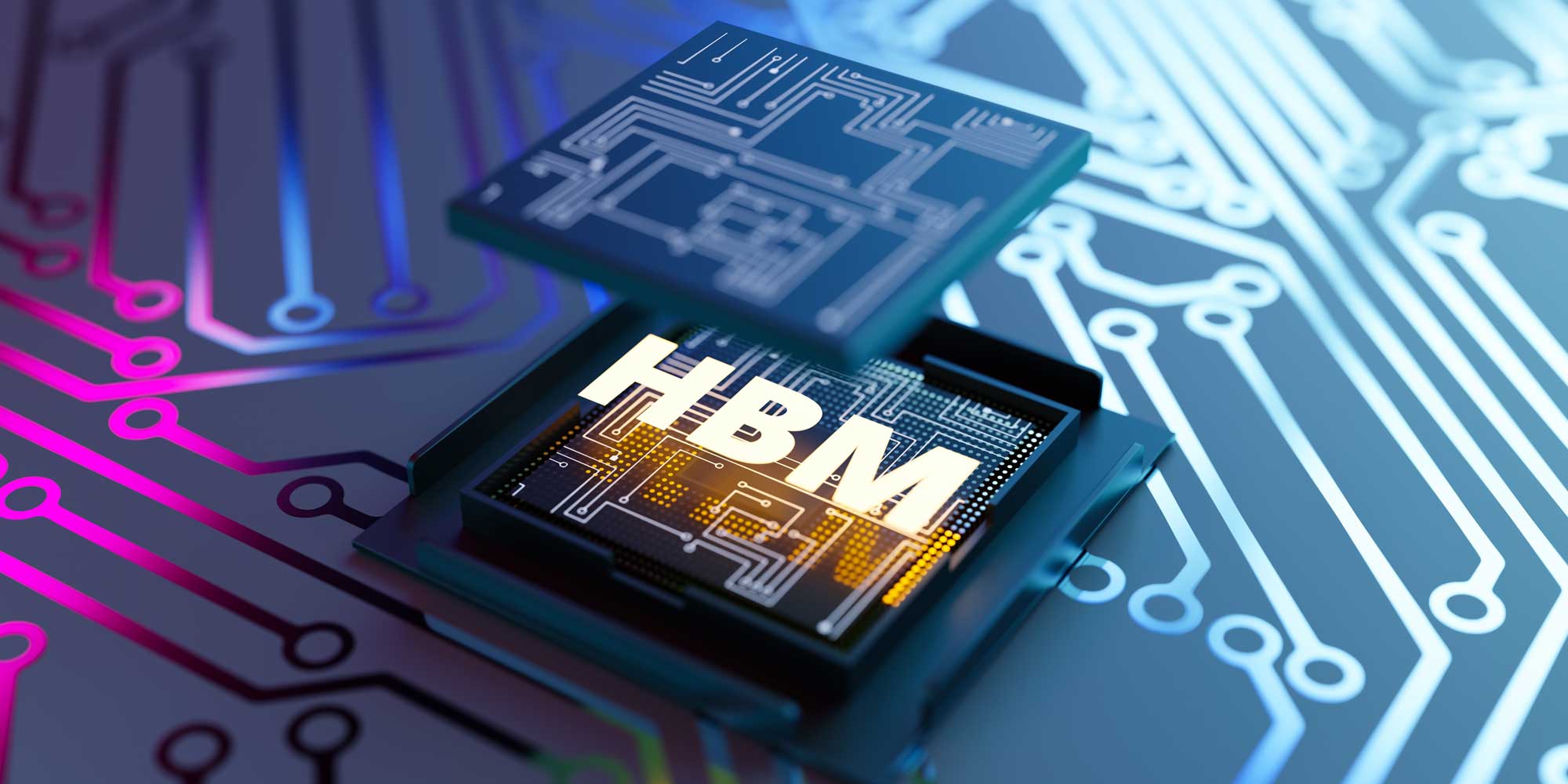
SK Hynix revealed plans for a new advanced packaging and test site, named P&T7, at the Cheongju Technopolis Industrial Park in Chungbuk, South Korea. The project carries a price tag of 19 trillion won (roughly $13 billion); ground work is slated to begin in April and SK targets finishing the facility by the end of 2027. The company says the site is intended to help meet rapidly rising demand for high-bandwidth memory (HBM), which is increasingly consumed by datacenter GPUs and AI accelerators. HBM production is complex: modules are created by stacking multiple DRAM layers (commonly eight to 12), and the process is sensitive to defects, making specialized packaging and testing critical. The announcement comes as SK prepares to bring its M15X DRAM fab online — a separate 20 trillion won project whose clean room opened in October and where equipment deployment is reportedly proceeding smoothly.
Why it matters
- P&T7 is aimed at expanding HBM output for datacenter GPUs and AI accelerators, easing pressure on AI infrastructure supply chains.
- Specialized packaging and test capacity is crucial because HBM stacks many DRAM layers and a single defect can void an expensive module.
- The new site aligns with SK Hynix’s broader capital investments (including the M15X DRAM fab) to scale memory production for AI demand.
- Despite added capacity for HBM, the facility is unlikely to materially reduce higher prices faced by consumer memory buyers in the near term.
Key facts
- Project name: P&T7 — an advanced packaging and test facility.
- Cost: 19 trillion Korean won (about $13 billion).
- Location: Cheongju Technopolis Industrial Park, Chungbuk, South Korea.
- Construction schedule: work begins in April; completion targeted by end of 2027.
- SK expects HBM demand to grow about 33% per year from 2025 through 2030.
- HBM production involves stacking multiple DRAM layers (eight and 12 layers are most common).
- HBM modules can reach data rates up to 2.75 TB/s in recent generations, requiring close co-packaging with compute logic.
- A single defect in a stacked HBM module can render the final product worthless, increasing the importance of packaging and test capacity.
- Related project: M15X DRAM fab (20 trillion won, ~ $13.5 billion) opened its clean room in October and is deploying equipment.
What to watch next
- Whether P&T7 meets SK Hynix’s timeline and begins production on schedule by late 2027.
- Impact of P&T7 on HBM supply for major buyers such as datacenter GPU and AI accelerator makers (AMD, Nvidia).
- Effect on broader DRAM and NAND pricing for consumers and businesses — not confirmed in the source.
Quick glossary
- High-Bandwidth Memory (HBM): A type of stacked DRAM designed for very high data throughput and energy efficiency, commonly used in datacenter GPUs and AI accelerators.
- Advanced packaging: Process steps that assemble and connect chips and memory stacks to enable high-performance, high-density modules.
- DRAM: Dynamic random-access memory, a common type of volatile memory used in computing devices for temporary data storage.
- DDR5: The fifth generation of double data rate synchronous DRAM used in modern PCs and servers.
Reader FAQ
What is P&T7 and where will it be built?
P&T7 is SK Hynix’s new advanced packaging and test facility to be built at Cheongju Technopolis Industrial Park in Chungbuk, South Korea.
When will construction and production start?
Work is scheduled to begin in April and SK targets completing the facility by the end of 2027.
Will this facility lower consumer memory prices?
The source says the new packaging site is unlikely to materially relieve the recent spike in consumer memory prices.
How much is SK Hynix investing in related DRAM capacity?
SK also developed the M15X DRAM plant, a separate 20 trillion won project whose clean room opened in October and is moving toward equipment deployment.
STORAGE SK Hynix's $13B packaging facility promises more HBM for the AI bubble Great news for AMD and Nvidia, less so for cash-strapped consumers Tobias Mann Tue 13 Jan 2026 // 19:22 UTC Memory…
Sources
- SK Hynix's $13B packaging facility promises more HBM for the AI bubble
- SK Hynix plans to open $13B HBM packaging plant in 2027
- SK hynix to spend $13 billion on new chip packaging facility in …
- SK Hynix plans $12.9b chip plant to meet demand
Related posts
- Sam Altman: From Tech Superstar to a Waning Influence in AI Era
- Trump: Americans shouldn’t ‘pick up the tab’ for AI datacenter grid upgrades
- Forrester: AI and automation could eliminate 10.4 million US jobs by 2030